Introduction
An example of a circuit that computes 35 different non-power-of-two DFT transform sizes used in the LTE SC-FDMA uplink protocol (12 to 1296 points) is described. It uses a single ROM memory to hold parameters that determine the specific factorizations and execution orderings used for loop index ranges in the verilog HDL coded control modules. Consequently, any transform size containing only the factors {2,3,4,5} can be computed and the number of different transform sizes that can be supported (including powers-of-2) is only limited by the size of this parameter memory.
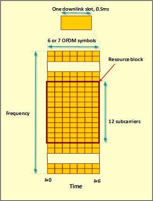
Here Centar’s LTE SC-FDMA circuit is compared to commercial designs also implemented in FPGA technologies. In order to provide a more relevant metric than throughput and latency numbers the length of time necessary to compute an LTE resource block (RB), as shown diagrammatically below, was chosen. The RB is the minimum processing unit of data for the LTE protocol and occupies one time “slot” (0.5ms), divided up into 7 symbols for (normal cyclic prefix). For example, 1296 subcarriers would imply processing a maximum of 108 RBs. This is a better performance comparison metric in that it requires both low latency and high throughput for good results.
Xilinx
A Vertix-6 (XC6VLX75T-3) FPGA was used as the target hardware for both the Xilinx and Centar’s circuit. The same software tools (ISE 14.7) for synthesis and place-and-route were also used. The Xilinx LogiCORE IP version 3.1 was used to generate a 16-bit version of their DFT because the SQNR of 60.0 db (average over all 35 transform sizes) was comparable to Centar’s 12-bit circuit with average SQNR=61.3. (Xilinx LogiCORE includes a bit accurate C model, callable as a Matlab mex function, that was used to obtain Xilinx SQNR values.)
The resource comparisons in the table below use a block RAM normalized to 18K bits, so that a 36K block RAM is considered equal to two 18K RAMs. Also, the “RB Average Throughput” column provides the average number of cycles (over all 35 DFT sizes) it takes to compute the DFT for the 7 symbols defined by a set of RBs as a function of the transform size N. Finally, the Fmax (maximum clock frequency) value and the number of DFT clock cycles are combined, providing a measure of the throughput, which is normalized to a value of “1” for the Centar design (a higher number is better). So the table shows the Xilinx circuit uses 41% more registers and 18% LUTs, while Centar circuits provides 37% higher throughput. So the overall combined gain is significant.
Since many wireless applications involve use of MIMO and cell towers can
have three different sectors operating simultaneously, it is possible that
more than one single carrier DFT cores could be required. In theory Centar’s
37% higher throughputs translate to fewer cores, which reduces considerably
the Xilinx advantage in block RAM usage shown in the table.
| Design | FPGA | LUT | Registers | Block RAM (9/18K) | Fmax (MHz) | RB Average Throughput (cycles) | Throughput (Normalized) |
| Centar | Virtex-6 | 2915 | 2581 | 19 | 401 | 16.6N | 1 |
| Xilinx | Virtex-6 | 3849 | 4326 | 10 | 403 | 23.4N | 0.72 |
| Centar | Stratix III | 3816 | 3188 | 29 | 400 | 16.6N | 1 |
| Intel | Stratix III | 2600 | N/A. | 17 | 260 | 32.9N | 0.33 |
Intel
Intel does not offer a DFT LTE core as does Xilinx; however, they have published results of an example design running on a Stratix III FPGA with 9K memory blocks that provides a useful basis for comparison.
For comparison the Centar design was also targeted to a Stratix III FPGA (EP3SE110F780C2) and the same Intel Quartus tools for synthesis and place-and-route were used to implement the design. The Intel implementation uses less logic, but is far slower, both in terms of the lower values of Fmax, and the increased number of cycles to complete the RB computation. Consequently, the Centar design has a significant ~3x higher throughput while LUT usage is only ~47% higher.
Note as well the Intel core doesn’t offer a 1296-point transform option and the outputs are not in normal order. Adding buffer circuitry to sort the output data would require additional logic and add ~N additional words of memory (~5 9K RAM blocks) to the numbers shown in the table.
To support several sectors with MIMO several Intel cores would need to
be used. In this case only one or two Centar cores would be required, so
that the Intel block RAM advantage shown in the table above would be
nullified, as shown in the table below. Here, the ratios are shown for each
of the elements, normalized to the design with the smaller resource
requirement for a particular element. As can be seen, except for the the
case of having just one sector and no more than two MIMO streams, the Centar
design uses significantly fewer LUTs and block RAMs, and slightly fewer
multipliers.
| Number MIMO Streams | Sectors | Total RB | Intel Cores Required | Centar Cores Required | LUT Intel::Centar | Block RAM Intel::Centar | Multipliers Intel::Centar |
| 1 | 1 | 1 | 1 | 1 | 1.00::1.47 | 1.00::1.32 | 1.00::1.875 |
| 2 | 1 | 2 | 1 | 1 | 1.00::1.47 | 1.00::1.32 | 1.00::1.875 |
| 4 | 1 | 4 | 2 | 1 | 1.36::1.00 | 1.52::1.00 | 1.07::1.00 |
| 1 | 3 | 3 | 2 | 1 | 1.36::1.00 | 1.52::1.00 | 1.07::1.00 |
| 2 | 3 | 6 | 3 | 1 | 2.04::1.00 | 2.27:1.00 | 1.60::1.00 |
| 4 | 3 | 12 | 4 | 2 | 1.36::1.00 | 1.52::1.00 | 1.07::1.00 |